On March 19, DOU Linyuan, an undergraduate of the Year 2018 from the Physics Experiment Base of Tongji University, published a paper “On-Chip Optical Beam Manipulation with an Electrically Tunable Lithium-Niobate-on-Insulator Metasurface” in Micromachines as the first author. Micromachines is an international, peer-reviewed open access journal which provides an advanced forum for studies related to micro-scaled machines and micromachinery. It is included in such databases as Scopus, SCIE (Web of Science) and PubMed.
Paper by DOU Linyuanas the first author in Micromachines
Compared with electronic integrated chips, photonic integrated chips have the advantages of faster information processing and transmission, and are safer and more efficient. They may become the technical core of the next generation of information revolution. Lithium niobate (LN) has attracted much attention because of its properties, e.g. broadband light transmittance, large refractive index, good nonlinear coefficient and excellent electro-optic effect. Therefore, LN has become a good choice for integrated photonics materials. DOU designed an electrically adjustable LNOI on-chip metasurface with the help of Gallop, an electromagnetic field simulation software, from their research group. The metasurface consists of 19 units, with a cuboid slit of 20 μm etched in the middle of each unit. The unit is 700 nm in width, and the device does not exceed 15 μm in width.
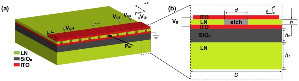
Figure 1. Schematic of the on-chip metasurface device. (a) Schematic of the three-dimensional structure of the on-chip metasurface device. The TE wave of wavelength λ = 1550 nm travels in the positive x direction (polarized in the y direction); (b) Schematic cross section of the device unit structure. The terms h = 0.5 μm, h1= 2 μm and h2 = 1 μm denote the thickness of the upper LN layer, lower LN layer, and silicon dioxide layer of LNOI, respectively. The cuboid slits etched in the upper LN layer are in the middle of the unit with a width of d = 70 nm.
On the chip, when the y-polarized light with a wavelength of 1550nm propagates to the metasurface along the positive x direction, most of the light will be bound in the cuboid slit, which is similar to the propagation in the waveguide. The simulation calculation of unit slit shows that when the bias voltage is not applied, the equal length cuboid slit will bring the same amount of phase in each unit. When different bias voltages are applied to each unit, the generated electric field will change the refractive index of LN constituting the slit waveguide, resulting in phase difference after light passes through the slit waveguide in each unit. The voltages applied in each unit are independent of each other; but due to the symmetry of the metasurface structure and the symmetry of the wavefront phase required to realize the intensity, the whole metasurface is controlled by nine continuously adjustable voltage groups, Δnomax represents the LN ordinary refractive index variation caused by the maximum voltage applied in all units under a certain metalens, the intensity of the metasurface and its dynamic adjustment.
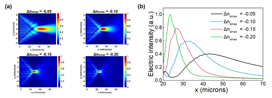
Figure 2. Focusing electric field intensity |Ey|2 distribution. (a) Electric field intensity |Ey|2 distribution in the x–y plane of metalens under different voltage groups; Δnomax shown at the top of each figure corresponds to the maximum ordinary refractive index variation due to the voltages applied in all units of the metalens; (b) Distribution of normalized electric field intensity of y = 0 cross section versus x coordinates in the metalens. The four curves Δnomax = −0.05, Δnomax = −0.10, Δnomax = −0.15 and Δnomax = −0.20 correspond to the metalens at the four voltage groups shown in (a), respectively.
On the premise of not changing the overall structure of the metasurface, changing the voltage applied to different units can also realize the adjustable polarization on the chip. The realization of deflection requires the electromagnetic wave front to be modulated into the phase of linear gradient. Only 9 units in the center of the metasurface can be used to apply the bias voltage of linear gradient. The figure below shows the on-chip electric field distribution when the metasurface realizes beam deflection at different angles |Ey|.
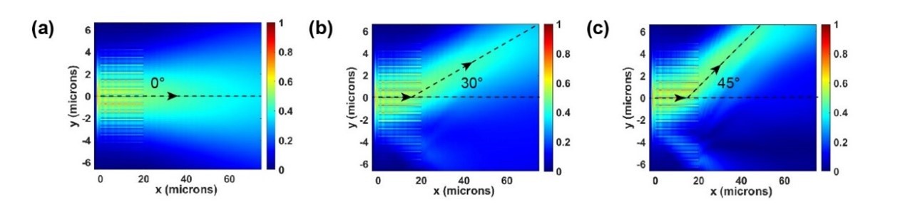
Figure 3. On-chip deflection realized by applying the linear gradient phase with designed voltages. (a) |Ey| with no voltages applied; (b) |Ey| when 30° on-chip deflection is realized. The maximum variation of the ordinary refractive index Δnomax = 0.0475 caused by the applied voltages; (c) |Ey| when 45° on-chip deflection is realized. The maximum variation of the ordinary refractive index Δnomax = 0.095 caused by the applied voltages.
The metasurface reported in this research realizes the adjustable focusing and deflection on LNOI chip. Its working wavelength is 1550nm, which realizes an adjustable simulation range at 23.41 μm~43.32 μm. The metalens can move about 19.9 μm under different voltage groups, about 13 incident wavelengths, which ensures the metalens efficiency of over 72%. When the beam deflects, it is adjustable in the range of 0 to 45°.
DOU started his research at the Research Group headed by Professor CHENG Xinbin and Professor WANG Zhanshan from the School of Physical Science and Engineering in August 2021. Under the guidance of WEI Zeyong, Associate Professor from the Institute of Precision Optics of Tongji University, he learned the basic theory and numerical simulation method of micro nano optics, and proposed a metasurface on lithium niobate (LNOI) on insulator. With the help of the metasurface, electrically tunable beam regulation functions such as focusing and deflection can be realized on LNOI chip. The corresponding authors of the paper are WEI Zeyong, and XIE Lingyun, postdoctoral student. The research was supported and funded by the National Natural Science Foundation of China, and Shanghai Digital Optics Frontier Science Base.
Link to paper:https://www.mdpi.com/2072-666X/13/3/472/htm
Source: https://news.tongji.edu.cn/info/1003/80515.htm